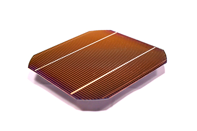
At the 25th European Photovoltaic Solar Energy Conference (Valencia, Spain), imec presents several large-area silicon solar cells with a conversion efficiency above 19%. Two types of cells were realized namely with Ag-screenprinted contacts and plated Cu-contacts.
Efficiencies of cells with screenprinted contacts were up to 19.1% whereas 19.4% was obtained with Cu-plated contacts. These high efficiencies were obtained thanks to several factors amongst which a combination of improved texturization and optimized firing conditions. The results were achieved on large-area cells (58,26 square inches) with 170µm thickness, proving the industrial viability of the process.
Imec’s record efficiency silicon solar cells feature rear-side passivation, laser ablation and, local aluminum back-side field and screen printed contacts or Cu-plated contacts on advanced emitter schemes.
“The fact that such efficiencies can be obtained by metallization schemes based on screen printed Ag contacts enables compatibility with present industrial metallization practice in the solar cell industry. The Cu-based front-side metallization is a step towards higher sustainability and lower cost, substituting Ag with Cu in future industrial production of crystalline silicon solar cells;” said Dr. Joachim John, team manager industrial solar cells at imec. “These exciting results were obtained in the new solar cell process facilities recently set up in imec.”
“High efficiency, low cost, and sustainability are the main drivers in imec’s research on crystalline silicon solar cells, eventually targeting cells that are only 40µm thick with efficiencies above 20. We expect further improvements towards efficiencies of up to 20% for large-area silicon solar cells. This achievement is a major step forward towards industrial manufacturing of sustainable, low-cost, thin silicon solar cells with high efficiency,” said Dr. Jef Poortmans, director imec energy/solar program.
The results were achieved within imec’s silicon solar cell industrial affiliation program (IIAP), a multi-partner R&D program that explores and develops advanced process technologies aiming a sharp reduction in silicon use, whilst increasing cell efficiency and hence further lowering substantially the cost per Watt peak.


Informative blog, saved the website for interest to read more information!