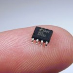
We are surrounded by nanoelectronics through products such as computers, mobile phones, sensors and electric cars.Nanoelectronics may also grow much stronger in the energy efficiency area in the near future. However, the sustainable growth faces several challenges.
In nanoelectronics, miniaturised electronic circuits are integrated on semiconductor chips where the basic element is the transistor. The size of the transistors produced is under 100 nm. Andreas Wild is Executive Director of the ENIAC JU. The task of this public-private partnership is to coordinate European research in nanoelectronics. He sees many interesting changes coming with the evolution of nanoelectronics.
“We have little electronics in the buildings, but the buildings are huge energy consumers. There will be an influx of nanoelectronics that will completely change the ways we are living in and using buildings, making them energy self-consistent, extremely comfortable and adaptable to the needs of the people. The buildings will be able to read how many people are inside, what are they doing, then adjust everything and also give the people a human interface to express their wishes. Rather than pilot projects this will be the norm. Europe has already issued regulations. I believe in the next five to ten years nobody will construct a building that haven’t got these features.”
Laurent Malier, CEO of the research centre CEA-Leti in France, highlights another area where nanoelectronics may be prominent. “What we are going to explore more are nanoelectronic devices for biology and healthcare. It could be easy and low cost diagnostics. This is an area of growth in a large perspective,” he said.
The sustainable growth of nanoelectronics faces several challenges. “You see technological challenges, materials, processes and so forth. You see design challenges, how to put together billions of components quickly, reliably and predictably. Then there are systemic challenges, what are the functions that all these billions of transistors are supposed to achieve on every chip and how do they relate to the everyday life of the people using the devices,” Wild said.
Malier sees additional challenges. “One is the compromise between low electrical power consumption and very fast processing capability. The other one is lithography, the capability to reduce the size of features. The third one is to increase complexity with either 3D integration, stacking chips on each other, or integration of new functions.”
We are dependent on nanoelectronic devices and soon we might see a drastic reduction in our energy consumption thanks to the advances in this area.


