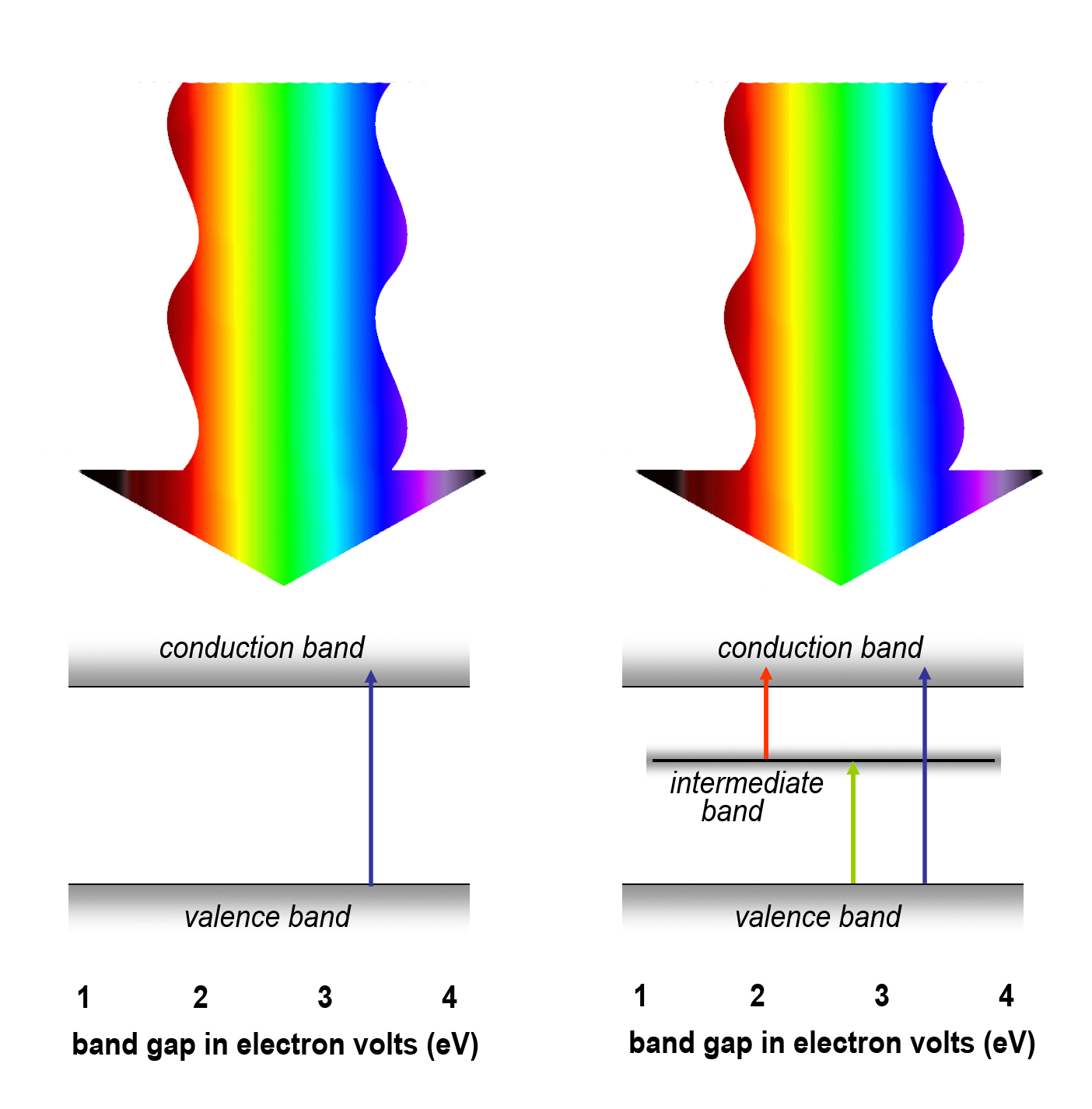
Solar cells are made from semiconductors whose ability to respond to light is determined by their band gaps (energy gaps). Different colors have different energies, and no single semiconductor has a band gap that can respond to sunlight’s full range, from low-energy infrared through visible light to high-energy ultraviolet.
Although full-spectrum solar cells have been made, none yet have been suitable for manufacture at a consumer-friendly price. Now Wladek Walukiewicz, who leads the Solar Energy Materials Research Group in the Materials Sciences Division (MSD) at the U.S. Department of Energy’s Lawrence Berkeley National Laboratory (Berkeley Lab), and his colleagues have demonstrated a solar cell that not only responds to virtually the entire solar spectrum, it can also readily be made using one of the semiconductor industry’s most common manufacturing techniques.
The new design promises highly efficient solar cells that are practical to produce. The results are reported in a recent issue of Physical Review Letters, available online to subscribers.
How to make a full-spectrum solar cell
“Since no one material is sensitive to all wavelengths, the underlying principle of a successful full-spectrum solar cell is to combine different semiconductors with different energy gaps,” says Walukiewicz.
One way to combine different band gaps is to stack layers of different semiconductors and wire them in series. This is the principle of current high-efficiency solar cell technology that uses three different semiconductor alloys with different energy gaps. In 2002, Walukiewicz and Kin Man Yu of Berkeley Lab’s MSD found that by adjusting the amounts of indium and gallium in the same alloy, indium gallium nitride, each different mixture in effect became a different kind of semiconductor that responded to different wavelengths. By stacking several of the crystalline layers, all closely matched but with different indium content, they made a photovoltaic device that was sensitive to the full solar spectrum.
However, says Walukiewicz, “Even when the different layers are well matched, these structures are still complex – and so is the process of manufacturing them. Another way to make a full-spectrum cell is to make a single alloy with more than one band gap.”
In 2004 Walukiewicz and Yu made an alloy of highly mismatched semiconductors based on a common alloy, zinc (plus manganese) and tellurium. By doping this alloy with oxygen, they added a third distinct energy band between the existing two – thus creating three different band gaps that spanned the solar spectrum. Unfortunately, says Walukiewicz, “to manufacture this alloy is complex and time-consuming, and these solar cells are also expensive to produce in quantity.”
The new solar cell material from Walukiewicz and Yu and their colleagues in Berkeley Lab’s MSD and RoseStreet Labs Energy, working with Sumika Electronics Materials in Phoenix, Arizona, is another multiband semiconductor made from a highly mismatched alloy. In this case the alloy is gallium arsenide nitride, similar in composition to one of the most familiar semiconductors, gallium arsenide. By replacing some of the arsenic atoms with nitrogen, a third, intermediate energy band is created. The good news is that the alloy can be made by metalorganic chemical vapor deposition (MOCVD), one of the most common methods of fabricating compound semiconductors.
How band gaps work
Band gaps arise because semiconductors are insulators at a temperature of absolute zero but inch closer to conductivity as they warm up. To conduct electricity, some of the electrons normally bound to atoms (those in the valence band) must gain enough energy to flow freely – that is, move into the conduction band. The band gap is the energy needed to do this.
When an electron moves into the conduction band it leaves behind a “hole” in the valence band, which also carries charge, just as the electrons in the conduction band; holes are positive instead of negative.
A large band gap means high energy, and thus a wide-band-gap material responds only to the more energetic segments of the solar spectrum, such as ultraviolet light. By introducing a third band, intermediate between the valence band and the conduction band, the same basic semiconductor can respond to lower and middle-energy wavelengths as well.
This is because, in a multiband semiconductor, there is a narrow band gap that responds to low energies between the valence band and the intermediate band. Between the intermediate band and the conduction band is another relatively narrow band gap, one that responds to intermediate energies. And finally, the original wide band gap is still there to take care of high energies.
“The major issue in creating a full-spectrum solar cell is finding the right material,” says Kin Man Yu. “The challenge is to balance the proper composition with the proper doping.”
In solar cells made of some highly mismatched alloys, a third band of electronic states can be created inside the band gap of the host material by replacing atoms of one component with a small amount of oxygen or nitrogen. In so—called II-VI semiconductors (which combine elements from these two groups of Mendeleev’s original periodic table), replacing some group VI atoms with oxygen produces an intermediate band whose width and location can be controlled by varying the amount of oxygen. Walukiewicz and Yu’s original multiband solar cell was a II-VI compound that replaced group VI tellurium atoms with oxygen atoms. Their current solar cell material is a III-V alloy. The intermediate third band is made by replacing some of the group V component’s atoms – arsenic, in this case – with nitrogen atoms.
Finding the right combination of alloys, and determining the right doping levels to put an intermediate band right where it’s needed, is mostly based on theory, using the band anticrossing model developed at Berkeley Lab over the past 10 years.
“We knew that two-percent nitrogen ought to do the job,” says Yu. “We knew where the intermediate band ought to be and what to expect. The challenge was designing the actual device.”
Passing the test
Using their new multiband material as the core of a test cell, the researchers illuminated it with the full spectrum of sunlight to measure how much current was produced by different colors of light. The key to making a multiband cell work is to make sure the intermediate band is isolated from the contacts where current is collected.
“The intermediate band must absorb light, but it acts only as a stepping stone and must not be allowed to conduct charge, or else it basically shorts out the device,” Walukiewicz explains.
The test device had negatively doped semiconductor contacts on the substrate to collect electrons from the conduction band, and positively doped semiconductor contacts on the surface to collect holes from the valence band. Current from the intermediate band was blocked by additional layers on top and bottom.
For comparison purposes, the researchers built a cell that was almost identical but not blocked at the bottom, allowing current to flow directly from the intermediate band to the substrate.
The results of the test showed that light penetrating the blocked device efficiently yielded current from all three energy bands – valence to intermediate, intermediate to conduction, and valence to conduction – and responded strongly to all parts of the spectrum, from infrared with an energy of about 1.1 electron volts (1.1 eV), to over 3.2 eV, well into the ultraviolet.
By comparison, the unblocked device responded well only in the near infrared, declining sharply in the visible part of the spectrum and missing the highest-energy sunlight. Because it was unblocked, the intermediate band had essentially usurped the conduction band, intercepting low-energy electrons from the valence band and shuttling them directly to the contact layer.
Further support for the success of the multiband device and its method of operation came from tests “in reverse” – operating the device as a light emitting diode (LED). At low voltage, the device emitted four peaks in the infrared and visible light regions of the spectrum. Primarily intended as a solar cell material, this performance as an LED may suggest additional possibilities for gallium arsenide nitride, since it is a dilute nitride very similar to the dilute nitride, indium gallium arsenide nitride, used in commercial “vertical cavity surface-emitting lasers” (VCSELs), which have found wide use because of their many advantages over other semiconductor lasers.
With the new, multiband photovoltaic device based on gallium arsenide nitride, the research team has demonstrated a simple solar cell that responds to virtually the entire solar spectrum – and can readily be made using one of the semiconductor industry’s most common manufacturing techniques. The results promise highly efficient solar cells that are practical to produce.


