Ultra-thin solar cells can absorb sunlight more efficiently than the thicker, more expensive-to-make silicon cells used today, because light behaves differently at scales around a nanometer (a billionth of a meter), say Stanford engineers. They calculate that by properly configuring the thicknesses of several thin layers of films, an organic polymer thin film could absorb as much as 10 times more energy from sunlight than was thought possible.
In the smooth, white, bunny-suited clean-room world of silicon wafers and solar cells, it turns out that a little roughness may go a long way, perhaps all the way to making solar power an affordable energy source, say Stanford engineers.
Their research shows that light ricocheting around inside the polymer film of a solar cell behaves differently when the film is ultra thin. A film that’s nanoscale-thin and has been roughed up a bit can absorb more than 10 times the energy predicted by conventional theory.
The key to overcoming the theoretical limit lies in keeping sunlight in the grip of the solar cell long enough to squeeze the maximum amount of energy from it, using a technique called “light trapping.” It’s the same as if you were using hamsters running on little wheels to generate your electricity – you’d want each hamster to log as many miles as possible before it jumped off and ran away.
“The longer a photon of light is in the solar cell, the better chance the photon can get absorbed,” said Shanhui Fan, associate professor of electrical engineering. The efficiency with which a given material absorbs sunlight is critically important in determining the overall efficiency of solar energy conversion. Fan is senior author of a paper describing the work published online this week by .Proceedings of the National Academy of Sciences
Light trapping has been used for several decades with silicon solar cells and is done by roughening the surface of the silicon to cause incoming light to bounce around inside the cell for a while after it penetrates, rather than reflecting right back out as it does off a mirror. But over the years, no matter how much researchers tinkered with the technique, they couldn’t boost the efficiency of typical “macroscale” silicon cells beyond a certain amount.
Eventually the scientists realized that there was a physical limit related to the speed at which light travels within a given material.
But light has a dual nature, sometimes behaving as a solid particle (a photon) and other times as a wave of energy, and Fan and postdoctoral researcher Zongfu Yu decided to explore whether the conventional limit on light trapping held true in a nanoscale setting. Yu is the lead author of the PNAS paper.
“We all used to think of light as going in a straight line,” Fan said. “For example, a ray of light hits a mirror, it bounces and you see another light ray. That is the typical way we think about light in the macroscopic world.
“But if you go down to the nanoscales that we are interested in, hundreds of millionths of a millimeter in scale, it turns out the wave characteristic really becomes important.”
Visible light has wavelengths around 400 to 700 nanometers (billionths of a meter), but even at that small scale, Fan said, many of the structures that Yu analyzed had a theoretical limit comparable to the conventional limit proven by experiment.
“One of the surprises with this work was discovering just how robust the conventional limit is,” Fan said.
It was only when Yu began investigating the behavior of light inside a material of deep subwavelength-scale – substantially smaller than the wavelength of the light – that it became evident to him that light could be confined for a longer time, increasing energy absorption beyond the conventional limit at the macroscale.
“The amount of benefit of nanoscale confinement we have shown here really is surprising,” said Yu. “Overcoming the conventional limit opens a new door to designing highly efficient solar cells.”
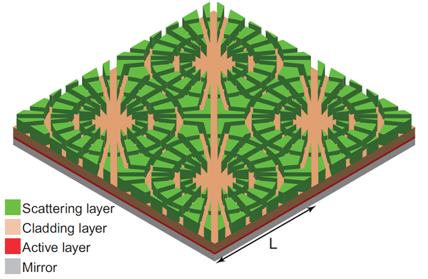
Yu determined through numerical simulations that the most effective structure for capitalizing on the benefits of nanoscale confinement was a combination of several different types of layers around an organic thin film.
He sandwiched the organic thin film between two layers of material – called “cladding” layers – that acted as confining layers once the light passed through the upper one into the thin film. Atop the upper cladding layer, he placed a patterned rough-surfaced layer designed to send the incoming light off in different directions as it entered the thin film.
By varying the parameters of the different layers, he was able to achieve a 12-fold increase in the absorption of light within the thin film, compared to the macroscale limit.
Nanoscale solar cells offer savings in material costs, as the organic polymer thin films and other materials used are less expensive than silicon and, being nanoscale, the quantities required for the cells are much smaller.
The organic materials also have the advantage of being manufactured in chemical reactions in solution, rather than needing high-temperature or vacuum processing, as is required for silicon manufacture.
“Most of the research these days is looking into many different kinds of materials for solar cells,” Fan said. “Where this will have a larger impact is in some of the emerging technologies; for example, in organic cells.”
“If you do it right, there is enormous potential associated with it,” Fan said.
Aaswath Raman, a graduate student in applied physics, also worked on the research and is a coauthor of the paper.
The project was supported by funding from the King Abdullah University of Science and Technology, which supports the Center for Advanced Molecular Photovoltaics at Stanford, and by the U.S. Department of Energy.


Well, you mention here things that really makes me think.
Hello! Is it okay if I go a bit off topic? I am trying to read your site on my Blackberry but it doesn’t display properly, any suggestions? Cheers! Darrin
You mention such a great things here and it is always pleassure to read. Hope to hear more and learn from you.